Modern Microprocessors
A 90-Minute Guide!
A brief, pulls-no-punches, fast-paced introduction to the main design aspects of modern processor microarchitecture.
Today's robots are very primitive, capable of understanding only a
few simple instructions such as 'go left', 'go right' and 'build car'.
WARNING: This article is meant to be informal and fun!
Okay, so you're a CS graduate and you did a hardware course as part of your degree, but perhaps that was a few years ago now, and you haven't really kept up with the details of processor designs since then.
In particular, you might not be aware of some key topics that developed rapidly in recent times...
- pipelining (superscalar, OOO, VLIW, branch prediction, predication)
- multi-core and simultaneous multi-threading (SMT, hyper-threading)
- SIMD vector instructions (MMX/SSE/AVX, AltiVec, NEON/SVE)
- caches and the memory hierarchy
Fear not! This article will get you up to speed fast. In no time, you'll be discussing the finer points of in-order vs out-of-order, hyper-threading, multi-core and cache organization like a pro.
But be prepared – this article is brief and to-the-point. It pulls no punches and the pace is pretty fierce (really). Let's get into it...
More Than Just Megahertz
The first issue that must be cleared up is the difference between clock speed and a processor's performance. They are not the same thing. Look at the results for processors of a few years ago (the late 1990s)...
| SPECint95 | SPECfp95 | ||
|---|---|---|---|
| 195 MHz | MIPS R10000 | 11.0 | 17.0 |
| 400 MHz | Alpha 21164 | 12.3 | 17.2 |
| 300 MHz | UltraSPARC | 12.1 | 15.5 |
| 300 MHz | Pentium II | 11.6 | 8.8 |
| 300 MHz | PowerPC G3 | 14.8 | 11.4 |
| 135 MHz | POWER2 | 6.2 | 17.6 |
Table 1 – Processor performance circa 1997.
A 200 MHz MIPS R10000, a 300 MHz UltraSPARC and a 400 MHz Alpha 21164 were all about the same speed at running most programs, yet they differed by a factor of two in clock speed. A 300 MHz Pentium II was also about the same speed for many things, yet it was about half that speed for floating-point code such as scientific number crunching. A PowerPC G3 at that same 300 MHz was somewhat faster than the others for normal integer code, but still far slower than the top three for floating-point. At the other extreme, an IBM POWER2 processor at just 135 MHz matched the 400 MHz Alpha 21164 in floating-point speed, yet was only half as fast for normal integer programs.
How can this be? Obviously, there's more to it than just clock speed – it's all about how much work gets done in each clock cycle. Which leads to...
Pipelining & Instruction-Level Parallelism
Instructions are executed one after the other inside the processor, right? Well, that makes it easy to understand, but that's not really what happens. In fact, that hasn't happened since the middle of the 1980s. Instead, several instructions are all partially executing at the same time.
Consider how an instruction is executed – first it is fetched, then decoded, then executed by the appropriate functional unit, and finally the result is written into place. With this scheme, a simple processor might take 4 cycles per instruction (CPI = 4)...
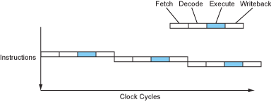
Figure 1 – The instruction flow of a sequential processor.
Modern processors overlap these stages in a pipeline, like an assembly line. While one instruction is executing, the next instruction is being decoded, and the one after that is being fetched...
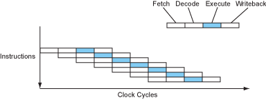
Figure 2 – The instruction flow of a pipelined processor.
Now the processor is completing 1 instruction every cycle (CPI = 1). This is a four-fold speedup without changing the clock speed at all. Not bad, huh?
From the hardware point of view, each pipeline stage consists of some combinatorial logic and possibly access to a register set and/or some form of high-speed cache memory. The pipeline stages are separated by latches. A common clock signal synchronizes the latches between each stage, so that all the latches capture the results produced by the pipeline stages at the same time. In effect, the clock "pumps" instructions down the pipeline.
At the beginning of each clock cycle, the data and control information for a partially processed instruction is held in a pipeline latch, and this information forms the inputs to the logic circuits of the next pipeline stage. During the clock cycle, the signals propagate through the combinatorial logic of the stage, producing an output just in time to be captured by the next pipeline latch at the end of the clock cycle...
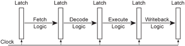
Figure 3 – A pipelined microarchitecture.
Since the result from each instruction is available after the execute stage has completed, the next instruction ought to be able to use that value immediately, rather than waiting for that result to be committed to its destination register in the writeback stage. To allow this, forwarding lines called bypasses are added, going backwards along the pipeline...
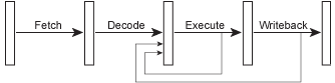
Figure 4 – A pipelined microarchitecture with bypasses.
Although the pipeline stages look simple, it is important to remember the execute stage in particular is really made up of several different groups of logic (several sets of gates), making up different functional units for each type of operation the processor must be able to perform...
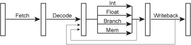
Figure 5 – A pipelined microarchitecture in more detail.
The early RISC processors, such as IBM's 801 research prototype, the MIPS R2000 (based on the Stanford MIPS machine) and the original SPARC (derived from the Berkeley RISC project), all implemented a simple 5-stage pipeline not unlike the one shown above. At the same time, the mainstream 80386, 68030 and VAX CISC processors worked largely sequentially – it's much easier to pipeline a RISC because its reduced instruction set means the instructions are mostly simple register-to-register operations, unlike the complex instruction sets of x86, 68k or VAX. As a result, a pipelined SPARC running at 20 MHz was way faster than a sequential 386 running at 33 MHz. Every processor since then has been pipelined, at least to some extent. A good summary of the original RISC research projects can be found in the 1985 CACM article by David Patterson.
Deeper Pipelines – Superpipelining
Since the clock speed is limited by (among other things) the length of the longest, slowest stage in the pipeline, the logic gates that make up each stage can be subdivided, especially the longer ones, converting the pipeline into a deeper super-pipeline with a larger number of shorter stages. Then the whole processor can be run at a higher clock speed! Of course, each instruction will now take more cycles to complete (latency), but the processor will still be completing 1 instruction per cycle (throughput), and there will be more cycles per second, so the processor will complete more instructions per second (actual performance)...
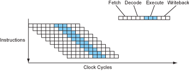
Figure 6 – The instruction flow of a superpipelined processor.
The Alpha architects in particular liked this idea, which is why the early Alphas had deep pipelines and ran at such high clock speeds for their era. Today, modern processors strive to keep the number of gate delays down to just a handful for each pipeline stage, about 12-25 gates deep (not total!) plus another 3-5 for the latch itself, and most have quite deep pipelines...
| Pipeline Depth | Processors |
|---|---|
| 6 | UltraSPARC T1 |
| 7 | PowerPC G4e |
| 8 | UltraSPARC T2/T3, Cortex-A9 |
| 9 | Cortex-X3 |
| 10 | Athlon, Scorpion, Cortex-X2 & X4 |
| 11 | Krait, Cortex-A73, Cortex-A77/A78 & X1 |
| 12 | Pentium Pro/II/III, Athlon 64, Apple A6 |
| 13 | Denver |
| 14 | UltraSPARC III/IV, Core 2, Apple A7/A8 |
| 14/19 | Sandy/Ivy Bridge, Haswell/Broadwell, Skylake |
| ~14/19 | Sunny/Golden Cove |
| 15 | Cortex-A15/A57, Cortex-A72 |
| 16 | PowerPC G5, Nehalem |
| ~17/19 | Zen 1-5 |
| 18 | Bulldozer, Steamroller |
| 20 | Pentium 4 |
| 31 | Pentium 4E Prescott |
Table 2 – Pipeline depths of common processors.
The x86 processors generally have deeper pipelines than the RISCs (of comparable era) because they need to do extra work to decode the complex x86 instructions (more on this later). UltraSPARC T1/T2/T3 Niagara are a recent exception to the deep-pipeline trend – just 6 for UltraSPARC T1 and 8 for T2/T3 to keep those cores as small as possible (more on this later, too).
Multiple Issue – Superscalar
Since the execute stage of the pipeline is really a bunch of different functional units, each doing its own task, it seems tempting to try to execute multiple instructions in parallel, each in its own functional unit. To do this, the fetch and decode/
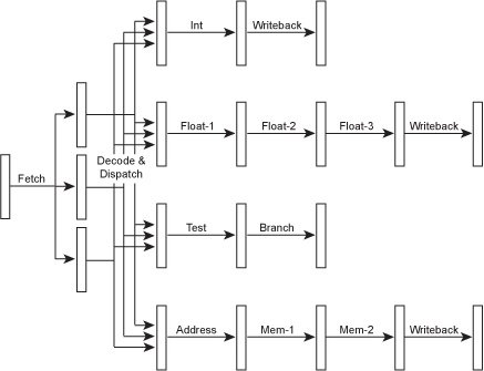
Figure 7 – A superscalar microarchitecture.
Of course, now that there are independent pipelines for each functional unit, they can even have different numbers of stages. This allows the simpler instructions to complete more quickly, reducing latency (which we'll get to soon). Since such processors have many different pipeline depths, it's normal to refer to the depth of a processor's pipeline when executing integer instructions, which is usually the shortest of the possible pipeline paths, with the memory and floating-point pipelines implied as having a few additional stages. Thus, a processor with a "10-stage pipeline" would use 10 stages for executing integer instructions, perhaps 12 or 13 stages for memory instructions, and maybe 14 or 15 stages for floating-point. There are also a bunch of bypasses within and between the various pipelines, but these have been left out of the diagram for simplicity.
In the above example, the processor could potentially issue 3 different instructions per cycle – for example 1 integer, 1 floating-point and 1 memory instruction. Even more functional units could be added, so that the processor might be able to execute 2 integer instructions per cycle, or 2 floating-point instructions, or whatever the target applications could best use.
On a superscalar processor, the instruction flow looks something like...
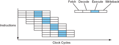
Figure 8 – The instruction flow of a superscalar processor.
This is great! There are now 3 instructions completing every cycle (CPI = 0.33, or IPC = 3, also written as ILP = 3 for instruction-level parallelism). The number of instructions able to be issued, executed or completed per cycle is called a processor's width.
Note that the issue width is less than the number of functional units – this is typical. There must be more functional units because different code sequences have different mixes of instructions. The idea is to execute 3 instructions per cycle, but those instructions are not always going to be 1 integer, 1 floating-point and 1 memory operation, so more than 3 functional units are required.
The IBM POWER1 processor, the predecessor of PowerPC, was the first mainstream superscalar processor. Most of the RISCs went superscalar soon after (SuperSPARC, Alpha 21064). Intel even managed to build a superscalar x86 – the original Pentium – however the complex x86 instruction set was a real problem for them (more on this later).
Of course, there's nothing stopping a processor from having both a deep pipeline and multiple instruction issue, so it can be both superpipelined and superscalar at the same time...
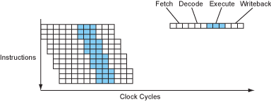
Figure 9 – The instruction flow of a superpipelined-superscalar processor.
Today, virtually every processor is a superpipelined-superscalar, so they're just called superscalar for short. Strictly speaking, superpipelining is just pipelining with a deeper pipe anyway.
The widths of modern processors vary considerably...
| Issue Width | Processors |
|---|---|
| 1 | UltraSPARC T1 |
| 2 | UltraSPARC T2/T3, Scorpion, Cortex-A9, Cortex-A73 |
| 3 | Pentium Pro/II/III/M, Pentium 4, Krait, Apple A6, Cortex-A15/A57, Cortex-A72 |
| 4 | UltraSPARC III/IV, PowerPC G4e, Kryo, Apple M1(E) |
| 4/8 | Bulldozer, Steamroller |
| 5 | PowerPC G5, Apple M2(E)-M4(E), Gracemont |
| 6 | Athlon, Athlon 64, Core 2, Nehalem, Sandy/Ivy Bridge, Apple A7-A10, Zen 1-4, Cortex-A77/A78, Apple M5(E) |
| 7 | Denver, Apple A11-A12 & M5(P) |
| 8 | Haswell/Broadwell, Skylake, Apple A13-A16 & M1(P)-M2(P), Cortex-X1-X3, Snapdragon X, Zen 5 |
| 9 | Apple M3(P), Snapdragon X2 |
| 10 | Sunny Cove, Apple M4(P)-M5(S), Cortex-X4-X925 |
| 12 | Golden Cove |
Table 3 – Issue widths of common processors.
The exact number and type of functional units in each processor depends on its target market. Some processors have more floating-point execution resources (IBM's POWER line), others are more integer-biased (Pentium Pro/II/III/M), some devote much of their resources to SIMD vector instructions (PowerPC G4/G4e), while most try to take the "balanced" middle ground.
Explicit Parallelism – VLIW
In cases where backward compatibility is not an issue, it is possible for the instruction set itself to be designed to explicitly group instructions to be executed in parallel. This approach eliminates the need for complex dependency-checking logic in the dispatch stage, which should make the processor easier to design, smaller, and easier to ramp up the clock speed over time (at least in theory).
In this style of processor, the "instructions" are really groups of little sub-instructions, and thus the instructions themselves are very long, often 128 bits or more, hence the name VLIW – very long instruction word. Each instruction contains information for multiple parallel operations.
A VLIW processor's instruction flow is much like a superscalar, except the decode/
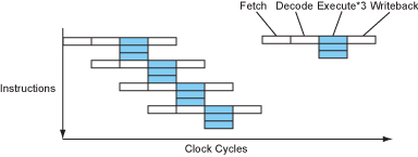
Figure 10 – The instruction flow of a VLIW processor.
Other than the simplification of the dispatch logic, VLIW processors are much like superscalar processors. This is especially so from a compiler's point of view (more on this later).
It is worth noting, however, that most VLIW designs are not interlocked. This means they do not check for dependencies between instructions, and often have no way of stalling instructions other than to stall the whole processor on a cache miss. As a result, the compiler needs to insert the appropriate number of cycles between dependent instructions, even if there are no instructions to fill the gap, by using nops (no-operations, pronounced "no ops") if necessary. This complicates the compiler somewhat, because it is doing something that a superscalar processor normally does at runtime, however the extra code in the compiler is minimal and it saves precious resources on the processor chip.
No VLIW designs have yet been commercially successful as mainstream CPUs, however Intel's failed IA-64 architecture and Itanium processors were once intended to be the replacement for x86. Intel chose to call IA-64 an "EPIC" design, for "explicitly parallel instruction computing", but it was essentially a VLIW with clever grouping (to allow long-term compatibility) and predication (see below). The programmable shaders in graphics processors (GPUs) are sometimes VLIW designs, as are many digital signal processors (DSPs), and there was also Transmeta (see the x86 section, coming up soon).
Instruction Dependencies & Latencies
How far can pipelining and multiple issue be taken? If a 5-stage pipeline is 5 times faster, why not build a 20-stage superpipeline? If 4-issue superscalar is good, why not go for 8-issue? For that matter, why not build a processor with a 50-stage pipeline which issues 20 instructions per cycle?
Well, consider the following two instructions...
a = b * c;
d = a + 1;
The second instruction depends on the first – the processor can't execute the second instruction until after the first has completed calculating its result. This is a serious problem, because instructions that depend on each other cannot be executed in parallel. Thus, multiple issue is impossible in this case.
If the first instruction was a simple integer addition, then this might still be okay in a pipelined single-issue processor, because integer addition is quick and the result of the first instruction would be available just in time to feed it back into the next instruction (using bypasses). However in the case of a multiply, which will take several cycles to complete, there is no way the result of the first instruction will be available when the second instruction reaches the execute stage just one cycle later. So, the processor will need to stall the execution of the second instruction until its data is available, inserting a bubble into the pipeline where no work gets done.
The number of cycles between when an instruction reaches the execute stage and when its result is available for use by other instructions is called the instruction's latency. The deeper the pipeline, the more stages and thus the longer the latency. So a very deep pipeline is not much more effective than a short one, because a deep one just gets filled up with bubbles thanks to all those nasty instructions depending on each other.
From a compiler's point of view, typical latencies in modern processors range from a single cycle for integer operations, to around 3-6 cycles for floating-point addition and the same or perhaps slightly longer for multiplication, through to over a dozen cycles for integer division.
Latencies for memory loads are particularly troublesome, in part because they tend to occur early within code sequences, which makes it difficult to fill their delays with useful instructions, and equally importantly because they are somewhat unpredictable – the load latency varies a lot depending on whether the access is a cache hit or not (we'll get to caches later).
Branches & Branch Prediction
Another key problem for pipelining is branches. Consider the following code sequence...
if (a > 7) {
    b = c;
} else {
    b = d;
}
...which compiles into something like...
    cmp a, 7    ; a > 7 ?
    ble L1
    mov c, b    ; b = c
    br L2
L1: mov d, b    ; b = d
L2: ...
Now consider a pipelined processor executing this code sequence. By the time the conditional branch at line 2 reaches the execute stage in the pipeline, the processor must have already fetched and decoded the next couple of instructions. But which instructions? Should it fetch and decode the if branch (lines 3 and 4) or the else branch (line 5)? It won't really know until the conditional branch gets to the execute stage, but in a deeply pipelined processor that might be several cycles away. And it can't afford to just wait – the processor encounters a branch every six instructions on average, and if it was to wait several cycles at every branch then most of the performance gained by using pipelining in the first place would be lost.
So the processor must make a guess. The processor will then fetch down the path it guessed and speculatively begin executing those instructions. Of course, it won't be able to actually commit (writeback) those instructions until the outcome of the branch is known. Worse, if the guess is wrong, the instructions will have to be cancelled, and those cycles will have been wasted. But if the guess is correct, the processor will be able to continue on at full speed.
The key question is how the processor should make the guess. Two alternatives spring to mind. First, the compiler might be able to mark the branch to tell the processor which way to go. This is called static branch prediction. It would be ideal if there was a bit in the instruction format in which to encode the prediction, but for older architectures this is not an option, so a convention can be used instead, such as backward branches are predicted to be taken while forward branches are predicted not-taken. More importantly, however, this approach requires the compiler to be quite smart in order for it to make the correct guess, which is easy for loops but might be difficult for other branches.
The other alternative is to have the processor make the guess at runtime. Normally, this is done by using an on-chip branch prediction table containing the addresses of recent branches and a bit indicating whether each branch was taken or not last time. In reality, most processors actually use two bits, so that a single not-taken occurrence doesn't reverse a generally taken prediction (important for loop back edges). Of course, this dynamic branch prediction table takes up valuable space on the processor chip, but branch prediction is so important that it's well worth it.
Unfortunately, even the best branch prediction techniques are sometimes wrong, and with a deep pipeline, many instructions might need to be cancelled. This is called the mispredict penalty. The Pentium Pro/II/III was a good example – it had a 12-stage pipeline and thus a mispredict penalty of 10-15 cycles. Even with a clever dynamic branch predictor that correctly predicted an impressive 90% of the time, this high mispredict penalty meant about 30% of the Pentium Pro/II/III's performance was lost due to mispredictions. Put another way, one third of the time, the Pentium Pro/II/III was not doing useful work but instead was saying "oops, wrong way".
Modern processors devote ever more hardware to branch prediction in an attempt to raise the prediction accuracy even further, and reduce this cost. Many record each branch's direction not just in isolation, but in the context of the couple of branches leading up to it, which is called a two-level adaptive predictor. Some keep a more global branch history, rather than a separate history for each individual branch, in an attempt to detect any correlations between branches even if they're relatively far away in the code. That's called a gshare or gselect predictor. The most advanced modern processors often implement several branch predictors and select between them based on which one seems to be working best for each individual branch!
Nonetheless, even the very best modern processors with the best, smartest branch predictors only reach a prediction accuracy of about 95-97%, and still lose quite a lot of performance due to branch mispredictions. The bottom line is simple – very deep pipelines naturally suffer from diminishing returns, because the deeper the pipeline, the further into the future you must try to predict, the more likely you'll be wrong, and the greater the mispredict penalty when you are.
Eliminating Branches with Predication
Conditional branches are so problematic that it would be nice to eliminate them altogether. Clearly, if statements cannot be eliminated from programming languages, so how can the resulting branches possibly be eliminated? The answer lies in the way some branches are used.
Consider the above example once again. Of the five instructions, two are branches, and one of those is an unconditional branch. If it was possible to somehow tag the mov instructions to tell them to execute only under some conditions, the code could be simplified...
cmp a, 7       ; a > 7 ?
mov c, b       ; b = c
cmovle d, b    ; if le, then b = d
Here, a new instruction has been introduced called cmovle, for "conditional move if less than or equal". This instruction works by executing as normal, but only commits itself if its condition is true (in the condition flags set by the most recent compare instruction). This is called a predicated instruction, because its execution is controlled by a predicate (a true/false test).
Given this new predicated move instruction, two instructions have been eliminated from the code, and both were costly branches. In addition, by being clever and always doing the first mov then overwriting it if necessary, the parallelism of the code has also been increased – lines 1 and 2 can now be executed in parallel, resulting in a 50% speedup (2 cycles rather than 3). Most importantly, though, the possibility of getting the branch prediction wrong and suffering a large mispredict penalty has been eliminated.
Of course, if the blocks of code in the if and else cases were longer, then using predication would mean executing more instructions than using a branch, because the processor is effectively executing both paths through the code. Whether it's worth executing a few more instructions to avoid a branch is a tricky decision – for very small or very large blocks the decision is simple, but for medium-sized blocks there are complex tradeoffs which the optimizer must consider.
The Alpha architecture had a conditional move instruction from the very beginning. MIPS, SPARC and x86 added it later. With IA-64, Intel went all-out and made almost every instruction predicated in the hope of dramatically reducing branching problems in inner loops, especially ones where the branches are unpredictable, such as compilers and OS kernels. Interestingly, the ARM architecture used in many phones and tablets was the first architecture with a fully predicated instruction set. This is even more intriguing given that the early ARM processors only had short pipelines and thus relatively small mispredict penalties.
Instruction Scheduling, Register Renaming & OOO
If branches and long-latency instructions are going to cause bubbles in the pipeline(s), then perhaps those empty cycles can be used to do other work. To achieve this, the instructions in the program must be reordered so that while one instruction is waiting, other instructions can execute. For example, it might be possible to find a couple of other instructions, from further down in the program, and put them between the two instructions in the earlier multiply example.
There are two ways to do this. One approach is to do the reordering in hardware at runtime. Doing dynamic instruction scheduling (reordering) in the processor means the dispatch logic must be enhanced to look at groups of instructions and dispatch them out of order as best it can to use the processor's functional units. Not surprisingly, this is called out-of-order execution, or just OOO for short (sometimes written OoO or OOE).
If the processor is going to execute instructions out of order, it will need to keep in mind the dependencies between those instructions. This can be made easier by not dealing with the raw architecturally-defined registers, but instead using a set of renamed registers. For example, a store of a register into memory, followed by a load of some other piece of memory into the same register, represent different values and need not go into the same physical register. Furthermore, if these different instructions are mapped to different physical registers, they can be executed in parallel, which is the whole point of OOO execution. So, the processor must keep a mapping of the instructions in flight at any moment and the physical registers they use. This process is called register renaming. As an added bonus, it becomes possible to work with a potentially larger set of real registers in an attempt to extract even more parallelism out of the code.
All of this dependency analysis, register renaming and OOO execution adds a lot of complex logic to the processor, making it harder to design, larger in terms of chip area, and more power-hungry. The extra logic is particularly power-hungry because those transistors are always working, unlike the functional units, which spend at least some of their time idle (possibly even powered down). On the other hand, out-of-order execution offers the advantage that software need not be recompiled to get at least some of the benefits of the new processor's design, though typically not all.
Another approach to the whole problem is to have the compiler optimize the code by rearranging the instructions. This is called static, or compile-time, instruction scheduling. The rearranged instruction stream can then be fed to a processor with simpler in-order multiple-issue logic, relying on the compiler to "spoon feed" the processor with the best instruction stream. Avoiding the need for complex OOO logic should make the processor quite a lot easier to design, less power-hungry, and smaller, which means more cores, or extra cache, could be placed onto the same amount of chip area (more on this later).
The compiler approach also has some other advantages over OOO hardware – it can see further down the program than the hardware, and it can speculate down multiple paths rather than just one, which is a big issue if branches are unpredictable. On the other hand, a compiler can't be expected to be psychic, so it can't necessarily get everything perfect all the time. Without OOO hardware, the pipeline will stall when the compiler fails to predict something like a cache miss.
Most of the early superscalars were in-order designs (SuperSPARC, hyperSPARC, UltraSPARC, Alpha 21064 & 21164, the original Pentium). Examples of early OOO designs included the MIPS R10000, Alpha 21264 and to some extent the entire POWER/
The Brainiac Debate
A question that must be asked is whether the costly out-of-order logic is really warranted, or whether compilers can do the task of instruction scheduling well enough without it. This is historically called the brainiac vs speed-demon debate. This simple (and fun) classification of design styles first appeared in a 1993 Microprocessor Report editorial by Linley Gwennap, and was made widely known by Dileep Bhandarkar's Alpha Implementations and Architecture book.
Brainiac designs are at the smart-machine end of the spectrum, with lots of OOO hardware trying to squeeze every last drop of instruction-level parallelism out of the code, even if it costs millions of logic transistors and years of design effort to do it. In contrast, speed-demon designs are simpler and smaller, relying on a smart compiler and willing to sacrifice a little bit of instruction-level parallelism for the other benefits that simplicity brings. Historically, the speed-demon designs tended to run at higher clock speeds, precisely because they were simpler, hence the "speed-demon" name, but today that's no longer the case because clock speed is limited mainly by power and thermal issues.
Clearly, OOO hardware should make it possible for more instruction-level parallelism to be extracted, because things will be known at runtime that cannot be predicted in advance – cache misses, in particular. On the other hand, a simpler in-order design will be smaller and use less power, which means you can place more small in-order cores onto the same chip as fewer, larger out-of-order cores. Which would you rather have: 8 powerful brainiac cores, or 32 simpler in-order cores, or perhaps 16 semi-brainiac cores?
Exactly which is the more important factor remains open to hot debate. In general, it seems both the benefits and the costs of OOO execution have been somewhat overstated in the past. In terms of cost, appropriate pipelining of the dispatch and register-renaming logic allowed OOO processors to achieve clock speeds competitive with simpler designs by the late 1990s, and clever engineering has reduced the power overhead of OOO execution considerably in recent years, leaving mainly the chip area cost. This is a testament to some outstanding engineering by processor architects.
Unfortunately, however, the effectiveness of OOO execution in dynamically extracting additional instruction-level parallelism has been disappointing, with only a relatively small improvement being seen, perhaps 20-40% or so over an equivalent in-order design. To quote Andy Glew, a pioneer of out-of-order execution and one of the chief architects of the Pentium Pro/II/III: "The dirty little secret of OOO is that we are often not very much OOO at all". Out-of-order execution has also been unable to deliver the degree of "recompile independence" originally hoped for, with recompilation still producing large speedups even on aggressive OOO processors.
When it comes to the brainiac debate, many vendors have gone down one path then changed their mind and switched to the other side...

Show Lineage:
Figure 11 – Brainiacs vs speed-demons.
DEC, for example, went primarily speed-demon with the first two generations of Alpha, then changed to brainiac for the third generation. MIPS did similarly, but starting 6 years earlier. Sun, on the other hand, went brainiac with their first superscalar SPARC, then switched to speed-demon for more recent designs. The POWER/
Intel have been the most interesting of all to watch. Modern x86 processors have no choice but to be at least somewhat brainiac, due to limitations of the x86 architecture (more on this soon), and the Pentium Pro embraced that sentiment wholeheartedly. Then the race against AMD to reach 1 GHz ensued, which AMD won by a nose in March 2000. Intel changed their focus to clock speed at all cost, and made the Pentium 4 about as speed-demon as possible for a decoupled x86 microarchitecture, sacrificing some ILP and using a deep 20-stage pipeline to pass 2 and then 3 GHz, and with a later revision featuring a staggering 31-stage pipeline, reach as high as 3.8 GHz. At the same time, with IA-64 Itanium (not shown above), Intel again bet solidly on the smart-compiler approach, with a simple design relying totally on static, compile-time scheduling. Faced with the failure of IA-64, the enormous power and heat issues of the Pentium 4, and the fact that AMD's more slowly clocked Athlon processors, in the 2 GHz range, were actually outperforming the Pentium 4 on real-world code, Intel then reversed their position once again, and revived the older Pentium Pro/II/III brainiac design to produce the Pentium M and its Core successors, which were a great success for many years. Recently, however, Intel once again faced thermal issues, this time due to falling behind in fabrication, having to extend Skylake to last 6 years and "backport" Sunny Cove to an older fab, with disappointing results.
The Power Wall & The ILP Wall
The Pentium 4's severe power and heat issues demonstrated there are limits to clock speed. It turns out power usage goes up even faster than clock speed does – for any given level of chip technology, increasing the clock speed of a processor by, say 20%, will typically increase its power usage by even more, maybe 50%, because not only are the transistors switching 20% more often, but the voltage also generally needs to be increased, in order to drive the signals through the circuits faster to reliably meet the shorter timing requirements, assuming the circuits work at all at the increased speed, of course. And while power increases linearly with clock frequency, it increases as the square of voltage, making for a kind of "triple whammy" at very high clock speeds (f*V*V).
It gets even worse, because in addition to the normal switching power, there is also a small amount of leakage power, since even when a transistor is off, the current flowing through it isn't completely reduced to zero. And just like the good, useful current, this leakage current also goes up as the voltage is increased. If that wasn't bad enough, leakage generally goes up as the temperature increases as well, due to the increased movement of the hotter, more energetic electrons within the silicon.
The net result is that today, increasing a modern processor's clock speed by a relatively modest 30% can take as much as double the power, and produce double the heat...
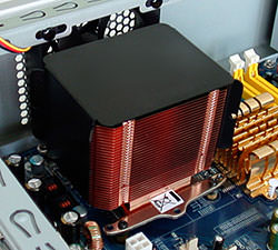
Figure 12 – The heatsink of a modern desktop processor, with front fan removed.
Up to a point, this increase in power is okay, but at a certain point, currently somewhere around 150-200 watts, the power and heat problems become unmanageable, because it's simply not possible to provide that much power and cooling to a silicon chip in any practical fashion, even if the circuits could, in fact, operate at higher clock speeds. This is called the power wall.
Processors which focused too much on clock speed, such as the Pentium 4, IBM's POWER6 and AMD's Bulldozer, quickly hit the power wall and found themselves unable to push the clock speed as high as originally hoped, resulting in them being beaten by slower-clocked but smarter processors which exploited more instruction-level parallelism.
Thus, going purely for clock speed is not the best strategy. And of course, this is even more true for portable, mobile devices, such as laptops, tablets and phones, where the power wall hits much sooner, around 50W for "pro" laptops, 15W for ultralight laptops, 10W for tablets and less than 5W for phones, due to the constraints of battery capacity and limited, often fanless cooling.
So, if going primarily for clock speed is a problem, is going purely brainiac the right approach then? Sadly, no. Pursuing more and more ILP also has definite limits, because unfortunately, normal programs just don't have a lot of fine-grained parallelism in them, due to a combination of load latencies, cache misses, branches and dependencies between instructions. This limit of available instruction-level parallelism is called the ILP wall.
Processors which focused too much on ILP, such as the early POWER processors, SuperSPARC and the MIPS R10000, soon found their ability to extract additional instruction-level parallelism was only modest, while the additional complexity seriously hindered their ability to reach fast clock speeds, resulting in those processors being beaten by dumber but higher-clocked processors which weren't so focused on ILP.
A 4-issue superscalar processor wants 4 independent instructions to be available, with all their dependencies and latencies met, at every cycle. In reality, this is virtually never possible, especially with load latencies of 3, 4 or 5 cycles. Currently, real-world instruction-level parallelism for mainstream, single-threaded applications is limited to about 2-3 instructions per cycle at best. In fact, the average IPC of a modern processor running the SPECint benchmarks is less than 2 instructions per cycle, and the SPEC benchmarks are somewhat "easier" than most large, real-world applications. Certain types of applications do exhibit more parallelism, such as scientific code, but these are generally not representative of mainstream applications. There are also some types of code, such as "pointer chasing", where even sustaining 1 instruction per cycle is extremely difficult. For those programs, the key problem is the memory system, and yet another wall, the memory wall (which we'll get to later).
What About x86?
So where does x86 fit into all this, and how have Intel and AMD been able to remain competitive through all of these developments, in spite of an architecture that's now more than 45 years old?
While the original Pentium, a superscalar x86, was an amazing piece of engineering, it was clear the big problem was the complex and messy x86 instruction set. Complex addressing modes and a minimal number of registers meant few instructions could be executed in parallel due to potential dependencies. For the x86 camp to compete with the RISC architectures, they needed to find a way to "get around" the x86 instruction set.
The solution, invented independently (at about the same time) by engineers at both NexGen and Intel, was to dynamically decode the x86 instructions into simple, RISC-like micro-instructions, which can then be executed by a fast, RISC-style register-renaming OOO superscalar core. The micro-instructions are usually called μops (pronounced "micro-ops"). Most x86 instructions decode into 1, 2 or 3 μops, while the more complex instructions require a larger number.
For these decoupled superscalar x86 processors, register renaming is absolutely critical due to the meager 8 registers of the x86 architecture in 32-bit mode (64-bit mode added an additional 8 registers, but even that's still not a lot). This differs strongly from the RISC architectures, where providing more registers via renaming only has a modest effect. Nonetheless, with clever register renaming, the full bag of RISC tricks become available to the x86 world, with the two exceptions of advanced static instruction scheduling (because the μops are hidden behind the x86 layer and thus are less visible to compilers) and the use of a large register set to avoid memory accesses.
The basic scheme works something like this...
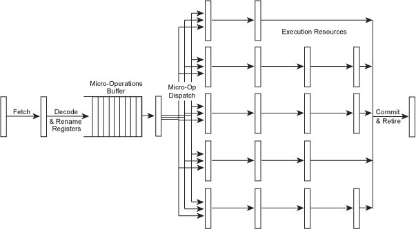
Figure 13 – A "RISCy x86" decoupled microarchitecture.
NexGen's Nx586 and Intel's Pentium Pro (also known as the P6) were the first processors to adopt a decoupled x86 microarchitecture design. Today, all modern x86 processors use this technique. Of course, they all differ in the exact design of their core pipelines, functional units and so on, just like the various RISC processors, but the fundamental idea of translating from x86 to internal μop RISC-like instructions is common to all of them.
Most of the more recent x86 processors even store the translated μops in a small buffer, or even a dedicated "L0" μop instruction cache, to avoid having to re-translate the same x86 instructions over and over again during loops, saving both time and power. That's why, for example, the pipeline depth of Core i*2/i*3 Sandy/Ivy Bridge was shown as 14/19 stages in the earlier section on superpipelining – it is 14 stages when the processor is running from its L0 μop cache (which is the common case), but 19 stages when running from the L1 instruction cache and having to decode x86 instructions and translate them into μops.
The decoupling of x86 instruction fetch and decode from internal RISC-like μop instruction dispatch and execution also makes defining the width of a modern x86 processor a bit tricky, and it gets even more unclear, because internally such processors often group or "fuse" μops into common pairs for ease of tracking (such as load-and-add or compare-and-branch). A processor such as Core i*4/i*5 Haswell/
One of the most interesting members of the RISC-style x86 group was the Transmeta Crusoe processor, which translated x86 instructions into an internal VLIW form, rather than internal superscalar, and used software to do the translation at runtime, much like a Java virtual machine or modern JavaScript JIT runtime. This approach allowed the processor itself to be a simple VLIW, without the complex x86 decoding and register-renaming hardware of decoupled x86 designs, and without any superscalar dispatch or OOO logic either. The software-based x86 translation did reduce the system's performance compared to hardware translation (which occurs as additional pipeline stages and thus is almost free in performance terms), but the result was a very lean chip which ran fast and cool and used very little power. A 600 MHz Crusoe processor could match a then-current 500 MHz Pentium III running in its low-power mode (300 MHz clock speed) while using only a fraction of the power and generating only a fraction of the heat. This made it ideal for laptops and handheld computers, where battery life is crucial. Today, of course, x86 processor variants designed specifically for low power use, such as the Pentium M and its Core descendants, have made the Transmeta-style software-based approach unnecessary, although a very similar approach was used in NVIDIA's Denver ARM processors, again in the quest for high performance at very low power.
Threads – SMT, Hyper-Threading & Multi-Core
As already mentioned, the approach of exploiting instruction-level parallelism through superscalar execution is seriously weakened by the fact that most normal programs just don't have a lot of fine-grained parallelism in them. Because of this, even the most aggressively brainiac OOO superscalar processor, coupled with a smart and aggressive compiler to spoon feed it, will still almost never exceed an average of about 2-3 instructions per cycle when running most mainstream, real-world software, due to a combination of load latencies, cache misses, branching and dependencies between instructions. Issuing many instructions in the same cycle only ever happens for short bursts of a few cycles at most, separated by many cycles of executing low-ILP code, so peak performance is not even close to being achieved.
If additional independent instructions aren't available within the program being executed, there is another potential source of independent instructions – other running programs, or other threads within the same program. Simultaneous multi-threading (SMT) is a processor design technique which exploits exactly this type of thread-level parallelism.
Once again, the idea is to fill those empty bubbles in the pipelines with useful instructions, but this time, rather than using instructions from further down in the same code (which are hard to come by), the instructions come from multiple threads running at the same time, all on the one processor core. So, an SMT processor appears to the rest of the system as if it were multiple independent processors, just like a true multi-processor system.
Of course, a true multi-processor system also executes multiple threads simultaneously – but only one in each processor. This is also true for multi-core processors, which place two or more processor cores onto a single chip, but are otherwise no different from traditional multi-processor systems. In contrast, an SMT processor uses just one physical processor core to present two or more logical processors to the system. This makes SMT much more efficient than a multi-core processor in terms of chip space, fabrication cost, power usage and heat dissipation. And of course there's nothing preventing a multi-core implementation where each core is an SMT design.
From a hardware point of view, implementing SMT requires duplicating all of the parts of the processor which store the "execution state" of each thread – things like the program counter, the architecturally-visible registers (but not the rename registers), the memory mappings held in the TLB, and so on. Luckily, these parts only constitute a tiny fraction of the overall processor's hardware. The really large and complex parts, such as the decoders and dispatch logic, the functional units, and the caches, are all shared between the threads.
Of course, the processor must also keep track of which instructions and which rename registers belong to which threads at any given point in time, but it turns out this only adds a small amount to the complexity of the core logic. So, for the relatively cheap design cost of around 10% more logic in the core, and an almost negligible increase in total transistor count and final production cost, the processor can execute several threads simultaneously, hopefully resulting in a substantial increase in functional-unit utilization and instructions per cycle, and thus overall performance.
The instruction flow of an SMT processor looks something like...
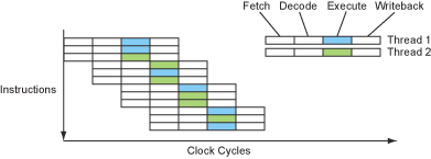
Figure 14 – The instruction flow of an SMT processor.
This is really great! Now that we can fill those bubbles by running multiple threads, we can justify adding more functional units than would normally be viable in a single-threaded processor, and really go to town with multiple instruction issue. In some cases, this may even have the side effect of improving single-thread performance (for particularly ILP-friendly code, for example).
So 20-issue here we come, right? Unfortunately, the answer is no.
SMT performance is a tricky business. First, the whole idea of SMT is built around the assumption that either lots of programs are simultaneously executing (not just sitting idle), or if just one program is running, it has lots of threads all executing at the same time. Experience with existing multi-processor systems shows this isn't always true. In practice, at least for desktops, laptops, tablets, phones and small servers, it is rarely the case that several different programs are actively executing at the same time, so it usually comes down to just the one task the machine is currently being used for.
Some applications, such as database systems, image and video processing, audio processing, 3D graphics rendering and scientific code, do have obvious high-level (coarse-grained) parallelism available and easy to exploit, but unfortunately even many of these applications have not been written to make use of multiple threads in order to exploit multiple processors. In addition, many of the applications which are easy to parallelize, because they're inherently "embarrassingly parallel" in nature, are primarily limited by memory bandwidth, not by the processor (image processing, audio processing, simple scientific code), so adding a second thread or processor won't help them much unless memory bandwidth is also dramatically increased (we'll get to the memory system soon). Worse yet, many other types of software, such as web browsers, multimedia design tools, language interpreters, hardware simulations and so on, are currently not written in a way which is parallel at all, or certainly not enough to make effective use of multiple processors.
On top of this, the fact that the threads in an SMT design are all sharing just one processor core, and just one set of caches, has major performance downsides compared to a true multi-processor (or multi-core). Within the pipelines of an SMT processor, if one thread saturates just one functional unit which the other threads need, it effectively stalls all of the other threads, even if they only need relatively little use of that unit. Thus, balancing the progress of the threads becomes critical, and the most effective use of SMT is for applications with highly variable code mixtures, so the threads don't constantly compete for the same hardware resources. Also, competition between the threads for cache space may produce worse results than letting just one thread have all the cache space available – particularly for software where the critical working set is highly cache-size sensitive, such as hardware simulators/emulators, virtual machines and high-quality video encoding (with a large motion-estimation window).
The bottom line is that without care, and even with care for some applications, SMT performance can actually be worse than single-thread performance and traditional context switching between threads. On the other hand, applications which are limited primarily by memory latency (but not memory bandwidth), such as database systems, 3D graphics rendering and a lot of general-purpose code, benefit dramatically from SMT, since it offers an effective way of using the otherwise idle time during load latencies and cache misses (we'll cover caches later). Thus, SMT presents a very complex and application-specific performance picture. This also makes it a difficult challenge for marketing – sometimes almost as fast as two "real" processors, sometimes more like two really lame processors, sometimes even worse than one processor, huh?
The Pentium 4 was the first processor to use SMT, which Intel calls "hyper-threading". Its design allowed for 2 simultaneous threads (although earlier revisions of the Pentium 4 had the SMT feature disabled due to bugs). Speedups from SMT on the Pentium 4 ranged from around -10% to +30% depending on the application(s). Subsequent Intel designs then eschewed SMT during the transition back to the brainiac designs of the Pentium M and Core 2, along with the transition to multi-core. Many other SMT designs were also cancelled around the same time (Alpha 21464, UltraSPARC V), and for a while it almost seemed as if SMT was out of favor, before it finally made a comeback with POWER5, a 2-thread SMT design as well as being multi-core (2 threads per core times 2 cores per chip equals 4 threads per chip). Intel's Core i series are also 2-thread SMT, so a typical quad-core Intel Core i processor is thus an 8-thread chip. Some of Intel's more recent Core Ultra processors dropped SMT, but it's slated to be reintroduced again in future generations. AMD's Zen processors also use 2-thread SMT. Sun was the most aggressive of all on the thread-level parallelism front, with UltraSPARC T1 Niagara providing 8 simple in-order cores each with 4-thread SMT, for a total of 32 threads on a single chip, a huge number at the time. This was subsequently increased to 8 threads per core in UltraSPARC T2, and then 16 cores per chip in UltraSPARC T3, for a whopping 128 threads!
More Cores or Wider Cores?
Given SMT's ability to convert thread-level parallelism into instruction-level parallelism, coupled with the advantage of better single-thread performance for particularly ILP-friendly code, you might now be asking why anyone would ever build a multi-core processor, when an equally wide (in total) SMT design would be superior.
Well unfortunately, it's not quite as simple as that. As it turns out, very wide superscalar designs scale very badly in terms of both chip area and clock speed. One key problem is that the complex multiple-issue dispatch logic scales up as roughly the square of the issue width, because all n candidate instructions need to be compared against every other candidate. Applying ordering restrictions or "issue rules" can reduce this, as can some clever engineering, but it's still in the order of n2. That is, the dispatch logic of a 5-issue processor is more than 50% larger than a 4-issue design, with 6-issue being more than twice as large, 7-issue over 3 times the size, and 8-issue more than 4 times larger than 4-issue – for only 2x the width, and far less than 2x the performance. In addition, a very wide superscalar design requires highly multi-ported register files and caches, to service all those simultaneous accesses. Both of these factors conspire to not only increase size, but also to massively increase the amount of longer-distance wiring at the circuit-design level, placing serious limits on the clock speed. So a single 10-issue core would actually be both larger and slower than two 5-issue cores, and our dream of a 20-issue SMT design isn't really viable due to circuit-design limitations.
Nevertheless, since the benefits of both SMT and multi-core depend so much on the nature of the target application(s), a broad spectrum of designs might still make sense with varying degrees of SMT and multi-core. Let's explore some possibilities...
Today, a "typical" SMT design implies both a wide execution core and OOO execution logic, including multiple decoders, the large and complex superscalar dispatch logic and so on. Thus, the size of a typical SMT core is quite large in terms of chip area. With the same amount of chip space, it would be possible to fit several simpler, single-issue, in-order cores (either with or without basic SMT). In fact, it may be the case that as many as half a dozen small, simple cores could fit within the chip area taken by just one modern OOO superscalar SMT design!
Now, given that both instruction-level parallelism and thread-level parallelism suffer from diminishing returns (in different ways), and remembering that SMT is essentially a way to convert TLP into ILP, but also remembering that wide superscalar designs scale very non-linearly in terms of chip area (and design complexity, and power usage), the obvious question is where is the sweet spot? How wide should the cores be made to reach a good balance between ILP and TLP? Right now, and for about the last decade and a half, many different approaches continue to be explored...
 |
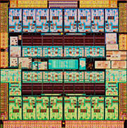 |
Figure 15 – Design extremes: Core i*2 "Sandy Bridge" vs UltraSPARC T3 "Niagara 3".
At one extreme, we have processors like Intel's Core i*2 Sandy Bridge (above left), which consisted of 4 large, wide, 6-issue, out-of-order, aggressively brainiac cores (along the top, with shared L3 cache below and integrated GPU on the left), each running 2 threads, for a total of 8 "fast" threads. At the other end of the spectrum, Sun/Oracle's UltraSPARC T3 Niagara 3 (above right) contained 16 much smaller, simpler, 2-issue in-order cores (top and bottom, with shared L2 cache towards the center), each running 8 threads, for a massive 128 threads in total, although these threads were considerably slower than those of Sandy Bridge. Both chips were from the same era – early 2011. Both contained around 1 billion transistors and are drawn approximately to scale above (assuming similar transistor density). Note just how much smaller the simple, in-order cores really are!
Which is the better approach? Alas, there's no simple answer here – once again it's going to depend very much on the application(s). For applications with lots of active but memory-latency-limited threads (database systems, 3D graphics rendering), more simple cores would be better, because big/
Of course, there are also a whole range of options between these two extremes that have (still) yet to be fully explored. IBM's POWER7, for example, was of the same generation, also having approximately 1 billion transistors, and used them to take the middle ground with an 8-core, 4-thread SMT design with moderately but not overly aggressive OOO execution hardware. AMD's Bulldozer design used a more unusual approach, with a shared, SMT-style front-end for each pair of cores, feeding a back-end with unshared, multi-core-style integer execution units but shared, SMT-style floating-point units, blurring the line between SMT and multi-core.
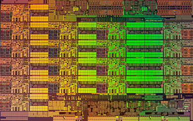
Figure 16 – Xeon Haswell with 18 brainiac cores, the best of both worlds?
A generation later (circa 2014), with several billion transistors now available thanks to Moore's Law, even aggressively brainiac designs could have quite a lot of cores – Intel's Xeon Haswell, the server version of Core i*4 Haswell, used 5.7 billion transistors to provide 18 cores (up from 8 in Xeon Sandy Bridge), each a very aggressively brainiac 8-issue design (up from 6-issue in Sandy Bridge), each still with 2-thread SMT, while IBM's POWER8 used 4.4 billion transistors to move to a considerably more brainiac core design than POWER7, and at the same time provide 12 cores (up from 8 in POWER7), each with 8-thread SMT (up from 4 in POWER7). Of course, whether such large, brainiac core designs are really an efficient use of all those transistors is a separate question.
Given the multi-core performance-per-area and performance-per-watt efficiency of small cores, but the maximum outright single-threaded performance of large cores, today we're seeing success with hybrid, mixed, asymmetric designs, with a few big, wide, brainiac cores plus an increasingly larger number of smaller, narrower, simpler cores. In many ways, such a design makes the most sense – highly parallel programs benefit from the many small cores more than a few large ones, but mostly single-threaded, sequential programs, which are still the dominant common case for most real-world end-users, want the might of at least one large, wide, brainiac core, even if it does take four or six times the area to provide only twice the single-threaded performance.
IBM's Cell processor (used in the Sony PlayStation 3) was arguably the first such design, but unfortunately it suffered from severe programmability problems, because the small, simple cores in Cell were not instruction-set compatible with the large main core and only had limited, awkward access to main memory, making them more like special-purpose coprocessors than general-purpose CPU cores. Many modern ARM designs also use an asymmetric approach, with several large cores along with some much smaller, simpler "companion" cores, not necessarily for maximum multi-core performance, but so that the large, power-hungry cores can be powered down if the phone or tablet is only being lightly used, to increase battery life – a strategy ARM calls "big.LITTLE".
Of course, with all of those transistors available, it might also make sense to integrate other secondary functionality into the main CPU chip, such as I/O and networking (usually part of the motherboard chipset), dedicated video encoding/
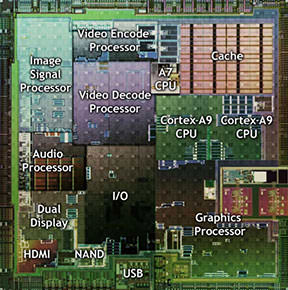
Figure 17 – An early SoC: NVIDIA Tegra 2.
Data Parallelism – SIMD Vector Instructions
In addition to instruction-level parallelism and thread-level parallelism, there is yet another source of parallelism in many programs – data parallelism. Rather than looking for ways to execute groups of instructions in parallel, the idea is to look for ways to make one instruction apply to a group of data values in parallel.
This is sometimes called SIMD parallelism (single instruction, multiple data). More often, it's called vector processing. Supercomputers used to use vector processing a lot, with very long vectors, because the types of scientific programs which are run on supercomputers are quite amenable to vector processing.
Today, however, vector supercomputers have long since given way to multi-processor designs where each processing unit is a commodity CPU. So why revive vector processing?
In many situations, especially in imaging, video and multimedia applications, a program needs to execute the same instruction for a small group of related values, usually a short vector (a simple structure or small array). For example, an image-processing application might want to add groups of 8-bit numbers, where each 8-bit number represents one of the red, green, blue or alpha (transparency) values of a pixel...
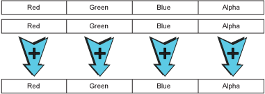
Figure 18 – A SIMD vector addition operation.
What's happening here is exactly the same operation as a 32-bit addition, except that every 8th carry is not being propagated. Also, it might be desirable for the values not to wrap to zero once all 8 bits are full, and instead to hold at 255 as a maximum value in those cases (called saturation arithmetic). In other words, every 8th carry is not carried across but instead triggers an all-ones result. So, the vector addition operation shown above is really just a modified 32-bit add.
From the hardware point of view, adding these types of vector instructions is not terribly difficult – existing registers can be used, and in many cases, the functional units can be shared with existing integer or floating-point units, with only minor modifications/
Of course, there's no reason to stop at 32 bits. If there happen to be some 64-bit registers, which most architectures usually have for floating-point (at least), they could be used to provide 64-bit vectors, thereby doubling the parallelism – SPARC VIS and x86 MMX did this. If it is possible to define entirely new registers, then they might as well be even wider – x86 SSE added 8 new 128-bit registers, later increased to 16 registers in 64-bit mode, then widened to 256 bits with AVX (and 512 bits with AVX-512), while POWER/PowerPC AltiVec provided a full set of 32 new 128-bit registers from the start (in keeping with POWER/PowerPC's more separated design style, where even the branch instructions have their own registers). An alternative to widening the registers is to use pairing, where each pair of registers is treated as a single operand by the SIMD vector instructions – ARM NEON does this, with its registers usable both as 32 64-bit registers or as 16 128-bit registers.
Naturally, the data in the registers can also be divided up in other ways, not just as 8-bit bytes – for example as 16-bit integers for high-quality image processing, or as floating-point values for scientific number crunching. With AltiVec, NEONv2 and recent versions of SSE/AVX, for example, it is possible to execute a 4-way parallel floating-point multiply-add as a single, fully pipelined instruction.
For applications where this type of data parallelism is available and easy to extract, SIMD vector instructions can produce amazing speedups. The original target applications were primarily in the area of image and video processing, however suitable applications also include audio processing, some parts of 3D graphics rendering, and many types of scientific code. For other types of software, such as compilers and database systems, the speedup is generally much smaller, perhaps even nothing at all.
Unfortunately, it's quite difficult for a compiler to automatically make use of vector instructions when working from normal source code, except in trivial cases. The key problem is that the way programmers write programs tends to serialize everything, which makes it difficult for a compiler to prove two given operations are independent and can be done in parallel. Progress is slowly being made in this area, but at the moment, programs must basically be rewritten by hand to take advantage of vector instructions (except for simple array-based loops in scientific code).
Luckily, however, rewriting just a small amount of code in key places within the graphics and video/
Almost every architecture has now added SIMD vector extensions, including SPARC (VIS), x86 (MMX/SSE/AVX), POWER/PowerPC (AltiVec) and ARM (NEON/SVE). Only relatively recent processors from each architecture can execute some of the newer instructions, however, which raises backward-compatibility issues, especially on x86 where the SIMD vector instructions evolved somewhat haphazardly (MMX, 3DNow!, SSE, SSE2, SSE3, SSE4, AVX, AVX2, AVX-512, AVX10). ARM, on the other hand, is transitioning to a much cleaner and less size-specific approach with its SVE "scalable" vector extensions, where the length is scalable from 128 up to 2048 bits, with binary compatibility, to allow increasing parallelism at the high-end, whilst also allowing low-end implementations on low-end processors.
Memory & The Memory Wall
As mentioned earlier, latency is a big problem for pipelined processors, and latency is especially bad for loads from memory, which make up about a quarter of all instructions.
Loads tend to occur near the beginning of code sequences (basic blocks), with most of the other instructions depending on the data being loaded. This causes all the other instructions to stall, and makes it difficult to obtain large amounts of instruction-level parallelism. Things are even worse than they might first seem, because in practice, most superscalar processors, even very wide ones, can still only issue 1, 2 or at the very most 3 load instructions per cycle.
The core problem with memory access is that building a fast memory system is very difficult, in part because of fixed limits like the speed of light, which impose delays while a signal is transferred out to RAM and back, and more importantly because of the relatively slow speed of charging and draining the tiny capacitors which make up the memory cells. Nothing can change these facts of nature – we must learn to work around them.
For example, access latency for main memory, using a good, modern DDR5 SDRAM with a CAS latency of just 30, will typically be 62 cycles of the memory system bus – 1 to send the command to the DIMM (memory module), RAS-to-CAS delay of 30 for the row access, CAS latency of 30 for the column access, and a final 1 to send the first piece of data up to the processor (or E-cache), with the remaining data block following over the next few bus cycles. Of course, that's just the typical latency, because memory latency varies quite a lot. For any given access, we might get lucky and be accessing a memory bank where the memory controller already has the right row open for us, skipping the RAS-to-CAS delay and saving nearly 50% of the latency (1+30+1), or we might be unlucky and access a bank where the memory controller has a row open but it's the wrong one, needing to first be put away, waiting an additional RAS precharge delay and adding nearly 50% to the latency (1+30+30+30+1, assuming the RAS-to-CAS and precharge latencies are also 30 like CAS, for the sake of simplicity). On a multi-processor system, even more bus cycles may be required to support cache coherency between the processors. And then there are the cycles within the processor itself, checking the various on-chip caches before the address even gets sent to the memory controller, and then when the data arrives from RAM to the memory controller and is sent to the relevant processor core. Luckily, those are faster internal CPU cycles, not memory bus cycles, but they still add up to another 30 CPU cycles or more in most modern processors.
Assuming a good, modern 3200 MHz SDRAM memory system (DDR5-6400) and assuming a 4 GHz processor, this makes (1+30+30+1) * 4000/3200 + 30 = 108 cycles of the CPU clock to access main memory! Yikes, you say! And it gets worse – a 4.5 GHz processor would take it to 118 cycles, a 5 GHz processor to 127 cycles, a 5.5 GHz processor 137 cycles, and a 6 GHz processor would wait a staggering 147 cycles to access main memory! And that's with very good memory and somewhat optimistic timings – many consumer systems have slower memory busses (DDR5-4800 or DDR5-5600) and use cheaper RAM with a longer CAS latency (sometimes up to 40), and thus can go well up over 200 cycles!
Older generations of processors were even worse, because their memory controllers weren't on-chip, but rather were part of the chipset on the motherboard, adding another 2 bus cycles for the transfer of the address and data between the processor and that motherboard chipset – and this was at a time when the memory bus was only 200 MHz or less, not 3200 MHz, so those 2 bus cycles often added another 20+ CPU cycles to the total. Some processors attempted to mitigate this issue by increasing the speed of their frontside bus (FSB) between the processor and the chipset (800 MHz QDR in Pentium 4, 1.25 GHz DDR in PowerPC G5). A far better approach, used by all modern processors, is to integrate the memory controller directly into the processor chip, which allows those 2 bus cycles to be converted into much faster CPU cycles instead. UltraSPARC IIi and Athlon 64 were the first mainstream processors to do this, while Intel were late to the party and only integrated the memory controller into their CPU chips starting with the Core i series.
Unfortunately, both DDR SDRAM memory and on-chip memory controllers are only able to do so much, and memory latency continues to be a major problem. This problem of the large, and slowly growing, gap between the processor and main memory is called the memory wall. It was, at one time, the single most important problem facing processor architects, although today the problem has eased considerably because processor clock speeds are no longer climbing at the rate they previously did, due to power and heat constraints – the power wall.
Nonetheless, the memory wall is still a big problem.
Caches & The Memory Hierarchy
Modern processors solve the problem of the memory wall with caches. A cache is a small but fast type of memory located on or near the processor chip. Its role is to keep copies of small pieces of main memory. When the processor asks for a particular piece of main memory, the cache can supply it much more quickly than main memory would be able to – if the data is in the cache.
Typically, there are small but fast "primary" level-1 (L1) caches on the processor chip itself, inside each core, usually around 8-64k in size, with a larger level-2 (L2) cache further away but still on-chip (a few hundred KB to a few MB), and possibly an even larger and slower L3 cache etc. The combination of the on-chip caches, any off-chip external cache (E-cache) and main memory (RAM) together form a memory hierarchy, with each successive level being larger but slower than the one before it. At the bottom of the memory hierarchy, of course, is virtual memory (paging/
It's a bit like working at a desk in a library... You might have two or three books open on the desk itself. Accessing them is fast (you can just look), but you can't fit more than a couple on the desk at the same time – and even if you could, accessing 100 books laid out on a huge desk would take longer because you'd have to walk between them. Instead, in the corner of the desk you might have a pile of a dozen more books. Accessing them is slower, because you have to reach over, grab one and open it up. Each time you open a new one, you also have to put one of the books already on the desk back into the pile to make room. Finally, when you want a book that's not on the desk, and not in the pile, it's very slow to access because you have to get up and walk around the library looking for it. However the size of the library means you have access to thousands of books, far more than could ever fit on your desk.
A typical modern memory hierarchy looks something like...
| Level | Size | Latency | Physical Location |
|---|---|---|---|
| L1 cache | 32 KB | 4 cycles | inside each core |
| L2 cache | 1 MB | 14 cycles | beside each core |
| L3 cache | 32 MB | ~49 cycles | shared between all cores |
| RAM | 4+ GB | 140+ cycles | SDRAM DIMMs on motherboard |
| Swap | 100+ GB | 10,000+ cycles | hard disk or SSD |
Table 4 – The memory hierarchy of a modern desktop/laptop: Zen 4.
Desktop computers, laptops, servers, tablets, phones and even microcontrollers all have a memory hierarchy like this, although the specific sizes and timings naturally differ. Lower-end devices often use slower, low-power RAM (LPDDR or similar), and phones and microcontrollers usually don't use any swap. Some high-end desktop systems, in contrast, and even some high-end laptops, add a large amount of extra cache as a separate piece of silicon, stacked and bonded directly onto the main CPU chip, to further increase cache size and avoid having to go out to slow main memory as often – AMD's 3D V-Cache chips are the most common example, popular with high-end gamers.
The amazing thing about caches is that they work really well – they effectively make the memory system seem almost as fast as the L1 cache, yet as large as main memory. A modern primary (L1) cache has a latency of just 3 to 5 processor cycles, which is dozens of times faster than accessing main memory, and modern primary caches achieve hit rates of around 90% for most software. So 90% of the time, accessing memory only takes a few cycles!
Caches can achieve these seemingly amazing hit rates because of the way programs work. Most programs exhibit locality in both time and space – when a program accesses a piece of memory, there's a good chance it will need to re-access the same piece of memory in the near future (temporal locality), and there's also a good chance it will need to access other nearby memory in the future as well (spatial locality). Temporal locality is exploited by merely keeping recently accessed data in the cache. To take advantage of spatial locality, data is transferred from main memory up into the cache in blocks of a few dozen bytes at a time, called a cache line.
From the hardware point of view, a cache works like a two-column table – one column is the memory address and the other is the block of data values (remember that each cache line is a whole block of data, not just a single value). Of course, in reality the cache need only store the necessary higher-end part of the address, since lookups work by using the lower part of the address to index the cache. When the higher part, called the tag, matches the tag stored in the table, that is a hit and the appropriate piece of data can be sent to the processor core...
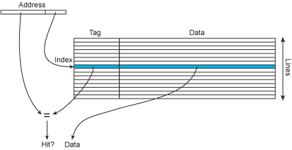
Figure 19 – A cache lookup.
It is possible to use either the physical address or the virtual address to do the cache lookup. Each has pros and cons (like everything else in computing). Using the virtual address might cause problems, because different programs use the same virtual addresses to map to different physical addresses – the cache might need to be flushed on every context switch. On the other hand, using the physical address means the virtual-to-physical mapping must be performed as part of the cache lookup, making every lookup slower. A common trick is to use virtual addresses for the cache indexing but physical addresses for the tags. The virtual-to-physical mapping (TLB lookup) can then be performed in parallel with the cache indexing, so that it will be ready in time for the tag comparison. Such a scheme is called a virtually-indexed physically-tagged cache.
The sizes and speeds of the various levels of cache in modern processors are absolutely crucial to performance. The most important by far are the primary L1 data cache (D-cache) and L1 instruction cache (I-cache). Some processors go for small L1 caches (Pentium 4E Prescott, Scorpion and Krait had 16k L1 caches (for each of I- and D-cache), earlier Pentium 4s and UltraSPARC T1/T2/T3 were even smaller at just 8k), most have settled on 32k as the sweet spot, and an increasing number are larger at 48k (Sunny/Golden Cove, Zen 5), or 64k (Athlon, Athlon 64, UltraSPARC III/IV, Apple A7-A11, Cortex-X1-X925), or 96k (Snapdragon X), or even 128k (Apple M1-M5, with a whopping 192k I-cache).
For modern L1 data caches, the load latency is usually 3 or 4 cycles (or 5 for Sunny/Golden Cove, sadly), depending on the processor's general clock-speed target range, but is occasionally shorter (2 cycles on UltraSPARC III/IV thanks to clock-less "wave" pipelining, 2 cycles in earlier processors due to their slower clock speeds and shorter pipelines, where a clock cycle was more real time). Increasing the load latency by a cycle, say from 3 to 4, or from 4 to 5, can seem like a minor change, but is actually a serious hit to performance, and is something rarely understood by end-users. For normal, everyday pointer-chasing code, a processor's load latency is a major factor in real-world performance.
Most modern processors have a large final level of cache, usually shared between all cores (and any integrated GPU). Whether this is an L2, L3, L4 or some external E-cache, as the last level of cache it's often written as LLC. This cache is very important, but its size sweet spot depends heavily on the type of application being run and the size of that application's active working set – the difference between 4 MB of LLC and 32 MB, or even 96+ MB with 3D V-Cache, will be barely measurable for some applications, while for others it will be enormous. Given that the relatively small L1 caches already take up a significant percentage of the chip area for many modern processor cores, you can imagine how much area a large LLC would take, yet this is still absolutely essential to combat the memory wall. Often, the large LLC takes as much as half the total chip area, so much that it's clearly visible in chip photographs, standing out as relatively clean, repetitive structures against the more "messy" logic transistors of the cores and memory controller (see earlier chip photos, above).
Large last-level caches have a long history of using interesting, advanced chip packaging technologies – anything to avoid going to slow main memory! The earliest large LLCs simply used separate, external cache chips (eg: SuperSPARC), but over the decades we've seen ever closer integration, from custom dual-chip packaging (Pentium Pro), to adjacent co-packaged eDRAM (Core i*4 Haswell), and most recently "3D" stacked, bonded silicon (Zen 3D V-Cache)...

Figure 20 – Evolution of large last-level cache packaging.
Advanced packaging is also sometimes used for CPU chips themselves, irrespective of large last-level caches, because using several smaller chips tightly packaged together helps increase yield, the percentage of chips on a wafer that operate correctly. A defect that kills only a single smaller so-called chiplet is less costly than that same defect killing a larger, full processor or SoC. It also allows the most advanced, expensive fabrication technology to be used only for the most important "compute" chiplets, not for less performance-critical I/O and other functionality that can get by with a generation or two older fabrication...

Figure 21 – One "chip" on the outside, 3 chiplets under the hood.
Of course, such a chiplet approach goes against the general long-term trend of more and more being integrated into the main CPU chip – first floating-point units in the 1980s, then large caches and memory controllers in the 1990s, then low-end GPUs in the 2000s, and entire SoC designs in the 2010s etc. So chiplets generally only make sense if either yields are a serious problem, usually due to a new, immature fabrication process, or if a processor is really pushing up against maximum size limits. Fabrication cost and fabrication process availability are also key factors, of course, which currently favor chiplets but may not stay that way in the long term. And of course, the packaging technology itself matters a great deal in terms of cost, performance and power use, with options ranging from simply placing multiple chiplets on a single very small board, to using a dedicated silicon substrate beneath the chiplets connecting them together (Intel's EMIB, TSMC's InFO_oS), to precision edge-to-edge bonding (the high-end of Apple's M series), or ideally multi-layer stacked designs (3D V-Cache, Foveros, various forms of HBM high-bandwidth memory).
Cache Conflicts & Associativity
Ideally, a cache should keep the data that is most likely to be needed in the future. Since caches aren't psychic, a good approximation of this is to keep the most recently used data.
Unfortunately, keeping exactly the most recently used data would mean that data from any memory location could be placed into any cache line. The cache would thus contain exactly the most recently used n KB of data, which would be great for exploiting locality but unfortunately is not suitable for allowing fast access – accessing the cache would require checking every cache line for a possible match, which would be very slow for a modern cache with hundreds of lines.
Instead, a cache usually only allows data from any particular address in memory to occupy one, or at most a handful, of locations within the cache. Thus, only one or a handful of checks are required during access, so access can be kept fast (which is the whole point of having a cache in the first place). This approach does have a downside, however – it means the cache doesn't store the absolutely best set of recently accessed data, because several different locations in memory will all map to the same one location in the cache. When two such memory locations are wanted at the same time, such a scenario is called a cache conflict.
Cache conflicts can cause "pathological" worst-case performance problems, because when a program repeatedly accesses two memory locations which happen to map to the same cache line, the cache must keep storing and loading from main memory and thus suffering the long main-memory latency on each access (100 cycles or more, remember!). This type of situation is called thrashing, since the cache is not achieving anything and is simply getting in the way – despite obvious temporal locality and reuse of data, the cache is unable to exploit the locality offered by this particular access pattern due to limitations of its simplistic mapping between memory locations and cache lines.
To address this problem, more sophisticated caches are able to place data in a small number of different places within the cache, rather than just a single place. The number of places a piece of data can be stored in a cache is called its associativity. The word "associativity" comes from the fact that cache lookups work by association – that is, a particular address in memory is associated with a particular location in the cache (or set of locations for a set-associative cache).
As described above, the simplest and fastest caches allow for only one place in the cache for each address in memory – each piece of data is simply mapped to address % size within the cache, by simply looking at the lower bits of the address (as in the above diagram). This is called a direct-mapped cache. Any two locations in memory whose addresses are the same for the lower address bits will map to the same cache line in a direct-mapped cache, causing a cache conflict.
A cache which allows data to occupy one of 2 locations based on its address is called 2-way set-associative. Similarly, a 4-way set-associative cache allows for 4 possible locations for any given piece of data, and an 8-way cache 8 possible locations. Set-associative caches work much like direct-mapped ones, except there are several tables, all indexed in parallel, and the tags from each table are compared to see whether there is a match for any one of them...
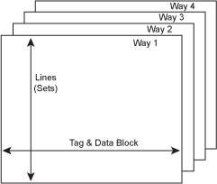
Figure 22 – A 4-way set-associative cache.
Each table, or way, may also have marker bits so that only the line of the least recently used way is evicted when a new line is brought in, or perhaps some faster approximation of that ideal.
Usually, set-associative caches are able to avoid the problems that occasionally occur with direct-mapped caches due to unfortunate cache conflicts. Adding even more ways allows even more conflicts to be avoided. Unfortunately, the more highly associative a cache is, the slower it is to access, because there are more operations to perform during each access. Even though the comparisons themselves are performed in parallel, additional logic is required to select the appropriate hit, if any, and the cache also needs to update the marker bits appropriately within each way. More chip area is also required, because relatively more of the cache's data is consumed by tag information rather than data blocks, and extra datapaths are needed to access each individual way of the cache in parallel. Any and all of these factors may negatively affect access time. Thus, a 2-way set-associative cache is slower but smarter than a direct-mapped cache, with 4-way and 8-way being slower but smarter again.
In most modern processors, the instruction cache can afford to be highly set-associative, because its latency is hidden somewhat by the fetching and buffering of the early stages of the processor's pipeline. The data cache, on the other hand, is usually set-associative to some degree, but not necessarily overly so, to minimize the all-important load latency. Most processors have settled on 4-way or 8-way as the sweet spot, but a few are less associative (2-way in Athlon, Athlon 64, PowerPC G5 & Cortex-A15/A57), and a handful are more associative (12-way in Sunny/Golden Cove and Zen 5). As the last resort before heading off to far-away main memory, the large LLC last-level cache is also usually highly associative, perhaps as much as 12- or 16-way, although external E-cache is sometimes direct-mapped for flexibility of size and implementation.
The concept of caches also extends up into software systems. For example, the operating system uses main memory to cache the contents of the filesystem to speed up file I/O, and web browsers cache recently viewed pages, images and JavaScript files in case you revisit those sites. With respect to main memory and virtual memory (paging/
Memory Bandwidth vs Latency
Since memory is transferred in blocks, and since cache misses are an urgent "show stopper" type of event with the potential to halt the processor in its tracks (or at least severely hamper its progress), the speed of those block transfers from memory is critical. The transfer rate of a memory system is called its bandwidth. But how is that different from latency?
A good analogy is a highway... Suppose you want to drive in to the city from 100 miles away. By doubling the number of lanes, the total number of cars that can travel per hour (the bandwidth) is doubled, but your own travel time (the latency) is not reduced. If all you want to do is increase cars-per-second, then adding more lanes (wider bus) is the answer, but if you want to reduce the time for a specific car to get from A to B then you need to do something else – usually either raise the speed limit (bus and RAM speed), or reduce the distance, or perhaps build a regional mall so that people don't need to go to the city as often (a cache).
When it comes to memory systems, there are often subtle tradeoffs between latency and bandwidth. Lower-latency designs will be better for pointer-chasing code, such as compilers and database systems, whereas bandwidth-oriented systems have the advantage for programs with simple, linear access patterns, such as image processing and scientific code. Of course, it's reasonably easy to increase bandwidth – simply adding more memory banks and making the busses wider can easily double or quadruple bandwidth. In fact, many high-end systems do this to increase their performance, but it comes with downsides as well. In particular, wider busses mean a more expensive motherboard, restrictions on the way RAM can be added to a system (install in pairs or groups of four) and a higher minimum RAM configuration.
Unfortunately, latency is much harder to improve than bandwidth – as the saying goes: "you can't bribe god". Even so, there have been some good improvements in effective memory latency in past years, chiefly in the form of synchronously clocked DRAM (SDRAM), which uses the same clock as the memory bus. The main benefit of SDRAM was that it allowed pipelining of the memory system, because the internal timing aspects and interleaved structure of SDRAM chip operation are exposed to the system and can thus be taken advantage of. This reduces effective latency because it allows a new memory access to be started before the current one has completed, thereby eliminating the small amounts of waiting time found in older asynchronous DRAM systems, which had to wait for the current access to complete before starting the next (on average, an asynchronous memory system had to wait for the transfer of half a cache line from the previous access before starting a new request, which was often several bus cycles, and we know how slow those were back then!).
In addition to the reduction in effective latency, there is also a substantial increase in bandwidth, because in an SDRAM memory system, multiple memory requests can be outstanding at any one time, all being processed in a highly efficient, fully pipelined fashion. Pipelining of the memory system has dramatic effects for memory bandwidth – an SDRAM memory system generally provided double or triple the sustained memory bandwidth of an asynchronous memory system of the same era, even though the latency of the SDRAM system was only slightly lower, and the same underlying memory-cell technology was in use (and still is).
Will further improvements in memory technology, along with even more levels of caching, plus "3D" chip stacking or other advanced packaging to add more cache and/or bring RAM closer, be able to continue to hold off the memory wall, while at the same time scaling up to the ever higher bandwidth demanded by more and more processor cores? Or will we soon end up constantly bottlenecked by memory, both bandwidth and latency, with neither the processor microarchitecture nor the number of cores making much difference, and the memory system being all that matters? It will be interesting to watch, and while predicting the future is never easy, there are good reasons to be optimistic...
Acknowledgments
The overall style of this article, particularly with respect to the style of the processor "instruction flow" and microarchitecture diagrams, is derived from a combination of a well-known 1989 ASPLOS paper by Norman Jouppi and David Wall, the book POWER and PowerPC by Shlomo Weiss and James Smith, and the two very famous Hennessy/Patterson textbooks Computer Architecture: A Quantitative Approach and Computer Organization and Design.
There have, of course, been many other presentations of this same material, and naturally they are all somewhat similar, however the above four are exceptionally good (in my opinion). To learn more about these topics, those books are an excellent place to start.
More Information?
If you want more detail on the specifics of recent processor designs, and something more insightful than the raw technical manuals, here are a few good articles...
- Apple Announces The Apple Silicon M1: Ditching x86 – the first of Apple's very successful M series, current leaders in single-threaded performance.
- AMD's Zen 4 – the fourth incremental upgrade of AMD's Zen microarchitecture, generally considered to be the current leader in x86 processors.
- Popping the Hood on Golden Cove – Intel's even wider, absolutely enormous x86 core, possibly taking things too far into diminishing returns?
- Gracemont: Revenge of the Atom Cores – the not-so-little efficiency core companion to Golden Cove (above), really its secret weapon for multi-core.
- The Qualcomm Snapdragon X Architecture Deep Dive – by far the most controversial CPU of recent times, in more ways than one!
- Skylake: Intel's Longest Serving Architecture – Intel's longest lived x86 processor design, an incremental step from Haswell that had to last 6 years.
- Intel's Haswell CPU Microarchitecture – the previous Intel x86 processor design, largely based on Sandy Bridge but with some notable upgrades.
- Intel's Sandy Bridge Microarchitecture – the most significant recent Intel x86 processor design, blending the Pentium Pro and Pentium 4 design styles.
- Intel's Merom Unveiled – Intel's revival of the venerable P6 core from the Pentium Pro/II/III/M to produce the long-running Core microarchitecture.
- The Pentium 4 and the PowerPC G4e (and Part II) – a comparison of the very different designs of two very successful, if somewhat maligned, processors.
- AMD's Bulldozer Microarchitecture – the novel resource-sharing approach used in AMD's Bulldozer, blurring the line between SMT and multi-core.
- The AMD Opteron Microprocessor (video) – introducing the Opteron/
Athlon 64 processor and AMD's 64-bit extensions to Intel's x86 architecture(!). - Into the K7 (and Part Two) – AMD's Athlon, the first competitor to topple Intel's position of leadership in the world of x86 processors.
- The microarchitecture of Intel, AMD, and VIA CPUs – detailed tech specs of the microarchitectures of nearly every x86 microprocessor.
- Niagara II: The Hydra Returns – Sun's innovative UltraSPARC T Niagara, revised for a second generation and taking thread-level parallelism to the extreme.
- Crusoe explored – the Transmeta Crusoe VLIW processor and its novel software-based approach to achieving (legal) x86 compatibility.
And here are some articles not specifically related to any particular processor, but still very interesting...
- Things CPU Architects Need To Think About (video) – an interesting presentation by Bob Colwell, one of the principle architects of the Pentium Pro/II/III.
- Designing an Alpha Microprocessor – a fascinating look at what really goes on in the various stages of a project to make a new processor.
- Understanding RAM: Timings, Frequency, and Performance – a deep dive into RAM frequency, internal organization, and how memory commands shape performance.
And if you want to keep up with the latest news in the world of microprocessors...
That should keep you busy!